Double Side PCB
Double Side PCB
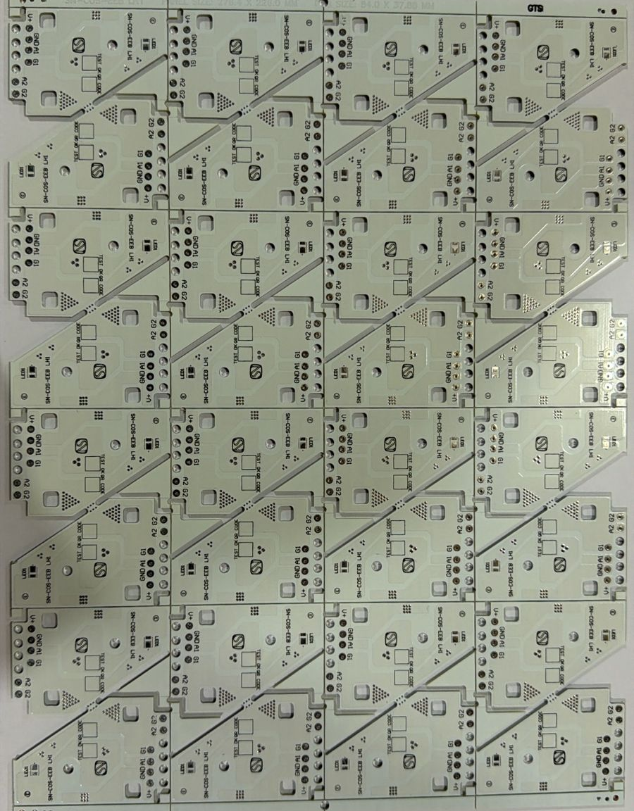
A Double-Side PCB (Printed Circuit Board) is an advanced type of circuit board that features conductive copper layers on both sides of the substrate, allowing for more complex and higher-density circuit designs. By utilizing both sides for component placement and routing, double-sided PCBs provide improved functionality while maintaining cost efficiency compared to multilayer boards.
Technical Specifications
- Base Material: FR-4 / High TG FR-4 / CEM-3 / Aluminium (optional)
- Copper Thickness: 1 oz – 4 oz (Top & Bottom)
- Board Thickness: 0.8mm – 3.2mm
- Layer Count: 2 Layers (Top & Bottom Copper)
- Minimum Hole Size: 0.3mm (Standard)
Copper Layers on Both Sides
Dual conductive copper layers enable circuit routing on both top and bottom surfaces for improved connectivity.
Plated Through-Hole Technology
Electrically connects both layers using vias, ensuring stable and reliable signal transmission.
Higher Component Density
Allows placement of more components within a compact space, supporting moderately complex circuit designs.
fa-diagram-project
Provides better routing flexibility and efficient space utilization compared to single-sided PCBs.